The heterogeneous integration of electronic devices has been drawing more interest for the demand of multi-functional integrated circuits (ICs) in future electronic system. The increasing popularity of internet of thing (IoT) applications call for the physical chip with the capabilities of environment sensing, data storage, signal processing and wireless transmission. Carbon nanotube has been considered as an emerging 1-D nano-material to construct high-performance complementary metal-oxide semiconductor (CMOS) filed-effect transistors (FETs) and circuits, and has shown the superiority in logic processing, advanced sensing, and millimeter-wave wireless communication. Notably, carbon nanotube-based sensors hold the potential in the fields of biological, chemical, gas, and other detections. The planar integrated sensor-interfacing circuits system has demonstrated the in situ sensing and processing for detecting such as environmental temperature and the sweat based on the silicon/ flexible substrates. Compared with the planar integration, the monolithic three-dimensional (M3D) architecture is the ideal technical support for sensor-memory-processor ICs: the interlayer dielectric/ via connections can protect the bottom circuitry and provide the low-latency, high-bandwidth communication approach. Furthermore, M3D fabrication meets the demand of compatible integration of memory layer and wireless transmission layer. In the previous reported works, the unmatured technology of carbon nanotube based M3D leads to the poor performance of system. And thus there is a lack of good demonstration of the CNT M3D sensing-processing system and ICs.
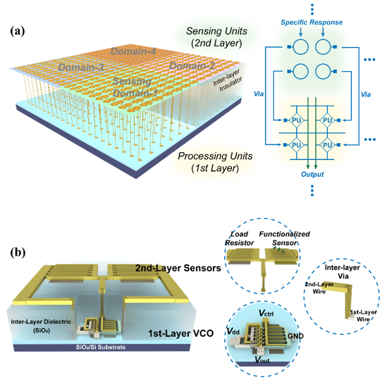
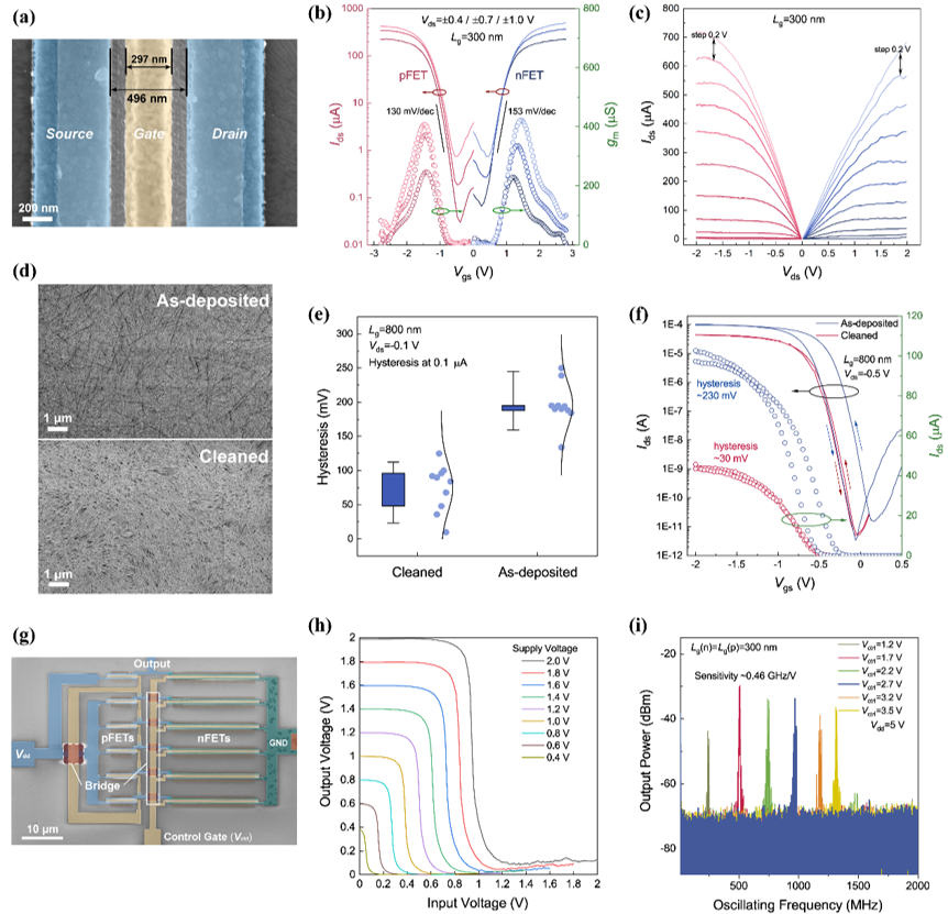
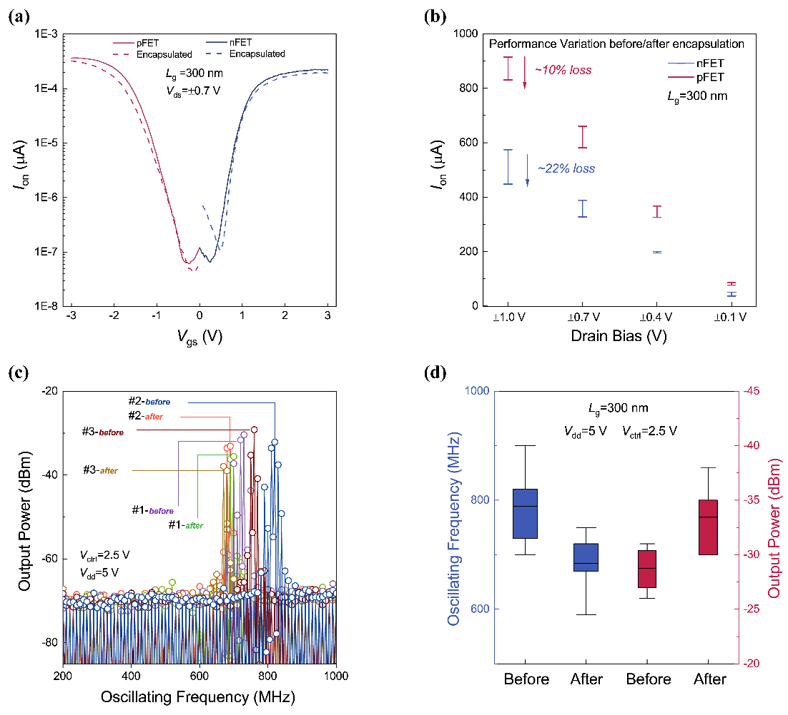
Recently, the research group of Prof. Zhiyong Zhang (School of Electronics; Carbon-Based Electronics Research Center, Peking University) employed the metal functionalized CNT FET as the upper-layer sensor units and the high-performance CMOS voltage-controlled oscillators (VCO) as the bottom interfacing/ signal converting units, realizing the M3D fully functional gas detection system (Fig. 1). By process optimization, the group demonstrated that the top-gated CMOS CNT FETs with gate length of 300 nm exhibited complementary driving capability, and thus constructed the uniform VCOs with voltage sensitivity of 0.46 GHz/V (Fig. 2). In this work, the effect of the M3D process on the stability of the bottom CMOS FETs and circuits has been explored, showing a frequency and power loss of the bottom VCOs less than 12%, 15%, respectively (Fig. 3). 48 carbon based M3D sensing systems were fabricated on a silicon substrate. In one system, CNT FETs with/without Pd modification served as the non-linear load resistor and hydrogen sensor, which could convert the conductance response to the continuous voltage under the H2 concentration from 8-128 ppm. The mid-voltage of the upper sensor stage adjusted the oscillating frequency, which served as the system output through the interlayer via. The M3D sensing system exhibited highly linear frequency-concentration response (r2=0.993) in real-time measurements for different H2 concentration conditions. The relative frequency response is larger than the conductance response of the upper sensor (Fig. 4). The M3D system can output a high-frequency response band of 0.78-1.11 GHz under Vdd of 5 V. With the Vdd downscaled to 3 V, the M3D sensing system shows a normal operation with lower active power consumption, which is prospective to build low-power, cross-sensitive CNT M3D gas detection system.
This research progress has been online published in ACS Nano entitled“Monolithic Three-Dimensional Integration of Carbon Nanotube Circuits and Sensors for Smart Sensing Chips”on May 31, 2023. Chenwei Fan, Ph. D. student (School of Electronics, Peking University) is the first author. Mengmeng Xiao, Assistant Research Scientist (Carbon-Based Electronics Research Center, Peking University) and Zhiyong Zhang, Professor (School of Electronics; Carbon-Based Electronics Research Center, Peking University) are the co-corresponding authors.
This research work is supported by the National Key Research & Development Program, the Natural Science Foundation of China, Beijing Science and Technology Program.
Full text: https://doi.org/10.1021/acsnano.3c03190

Figure 1. 3D schematics of carbon nanotube M3D sensing system.

Figure 2. Bottom-layer CNT CMOS transistors and circuits.

Figure 3. Performance variations in FETs and VCOs before and after M3D process.

Figure 4. Practical demonstration of the M3D H2sensing system.


