The development of integrated circuits relies on the scaling of transistor sizes for better electronic performance, higher integration density, less power consumption, and lower manufacturing cost. The scaling of silicon transistors is facing challenges in terms of power consumption, manufacturing cost, and physical limits as silicon CMOS technology reaches 5 nm technology node and below. Academia and industry both devote tremendous efforts to research potential electronic materials, device structures, and system architectures for the continuing development of integrated circuits. Among all these efforts, the most prominent one is to build transistors using semiconductors with ultrathin thickness and high carrier mobility for better scaling and higher electronic performance than silicon CMOS devices. Carbon nanotubes have great potential to outperform commercial silicon transistors, and have been set high expectations for next-generation digital integrated circuits. However, the majority of research efforts focus only on the scaling of gate length or channel length, which cannot truly reflect the scaling and integration potential of carbon nanotube transistors. Contacted gate pitch (CGP) is a key figure of merits to measure the integration density of transistors in industry. Transistors based on carbon nanotubes or other low-dimensional semiconductors reported so far by academia have much larger CGP (typically greater than 400 nm) which cannot be accepted for integrated circuits with billions of transistors. Therefore, it is crucial to explore the true potential of carbon nanotube transistors with a given CGP, and to propose key performance indicators for the technology nodes of carbon-nanotube-based electronics.
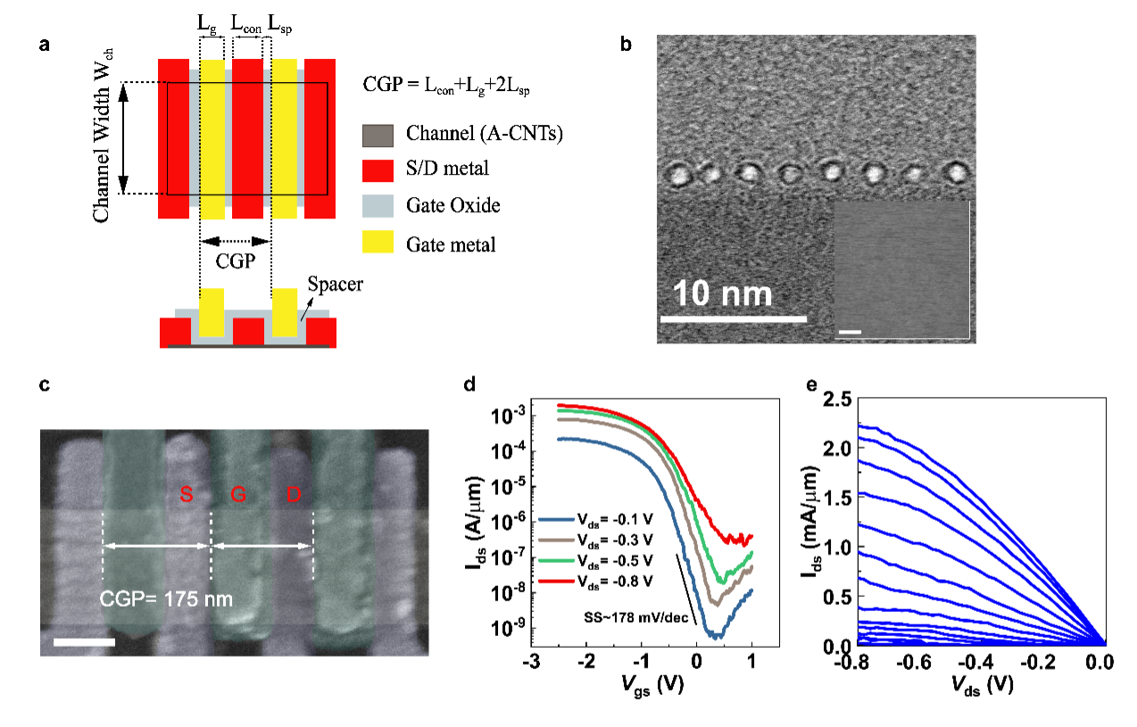
In this work, we demonstrated transistors and circuits based on aligned carbon nanotubes (A-CNTs) for 90 nm technology node for the first time, and explored the potential to scale these A-CNT transistors to sub-10 nm technology node. We fabricated transistors with a CGP of 175 nm by scaling the gate length and contact length to 85 nm and 80 nm, respectively, based on our previously developed wafer-scale high-density (~300 tubes/μm) and high semiconducting purity (99.9999%) A-CNTs (Science 368, 850, 2020).Remarkably, the A-CNT transistor exhibited an impressive on-current of 2.24 mA∙μm-1and a peak transconductance of 1.64 mS∙μm-1, surpassing silicon 45 nm node transistors in terms of both device size and electronic performance (Fig.1).

Figure 1. High performance A-CNT transistors for 90 nm technology node
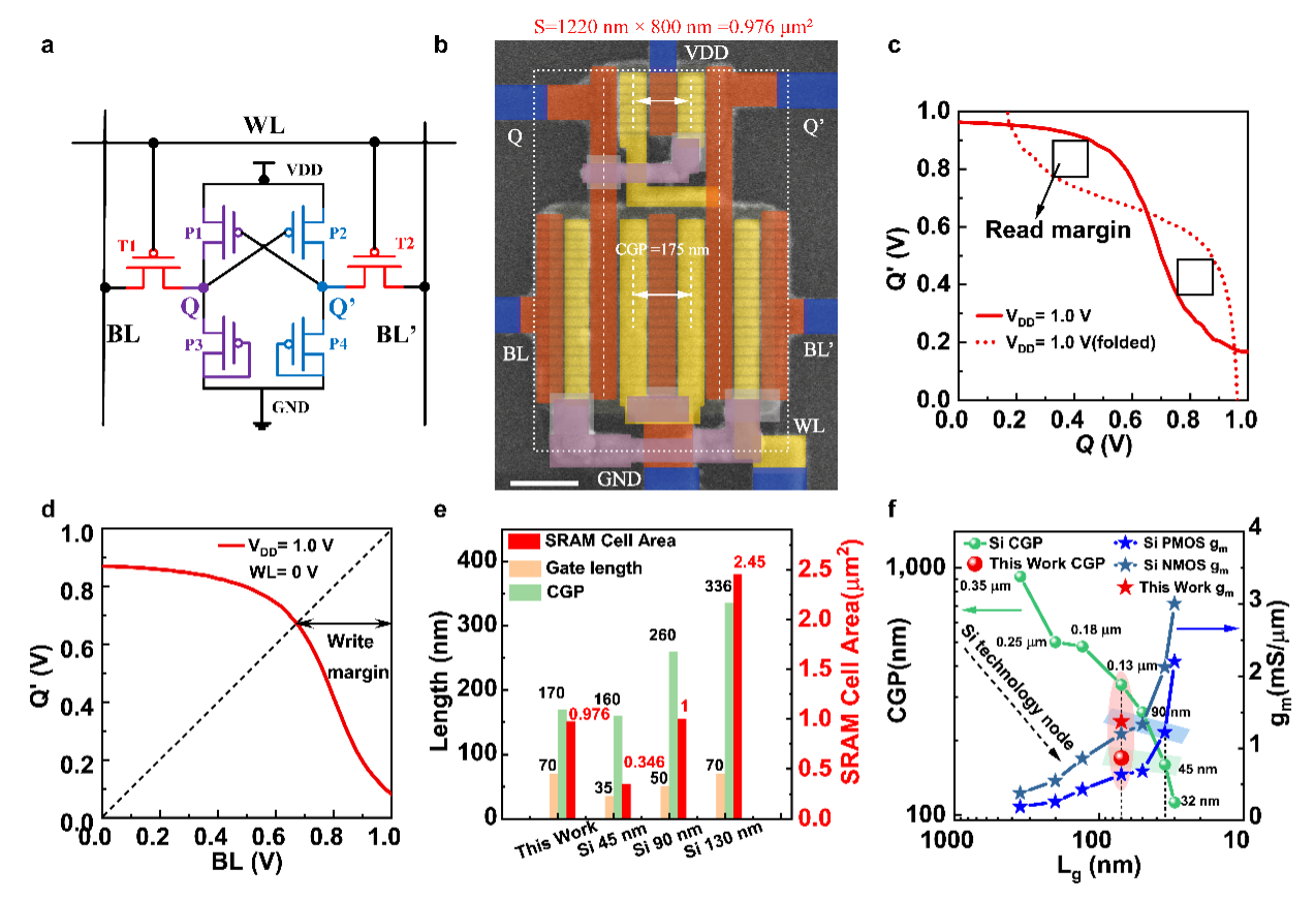
Furthermore, we showed a six-transistor (6T) static random-access memory (SRAM) cell by these ultra-scaled A-CNT FETs, demonstrating a total area (0.967 μm2) comparable to the 90 nm node (1 μm2) of silicon CMOS technology (Fig.2).

Figure 2. Ultrascaled A-CNT 6T-SRAM cell for 90 nm technology node
The area of 6T SRAM cell is another key figure of merits to measure the integration density in silicon integrated circuits as the cache, consisting of 6T SRAM cells, occupies large area of a central processing unit (CPU). The previously reported 6T SRAM cells based on carbon nanotubes or other low-dimensional semiconductors all have areas greater than 2000 μm2, much larger than that of silicon 90 nm technology node. Our work demonstrated functional 6T SRAM cells with an area less than 1 μm2based on non-silicon materials for the first time, manifesting that carbon nanotube digital electronics could satisfy the requirements of 90 nm technology node.
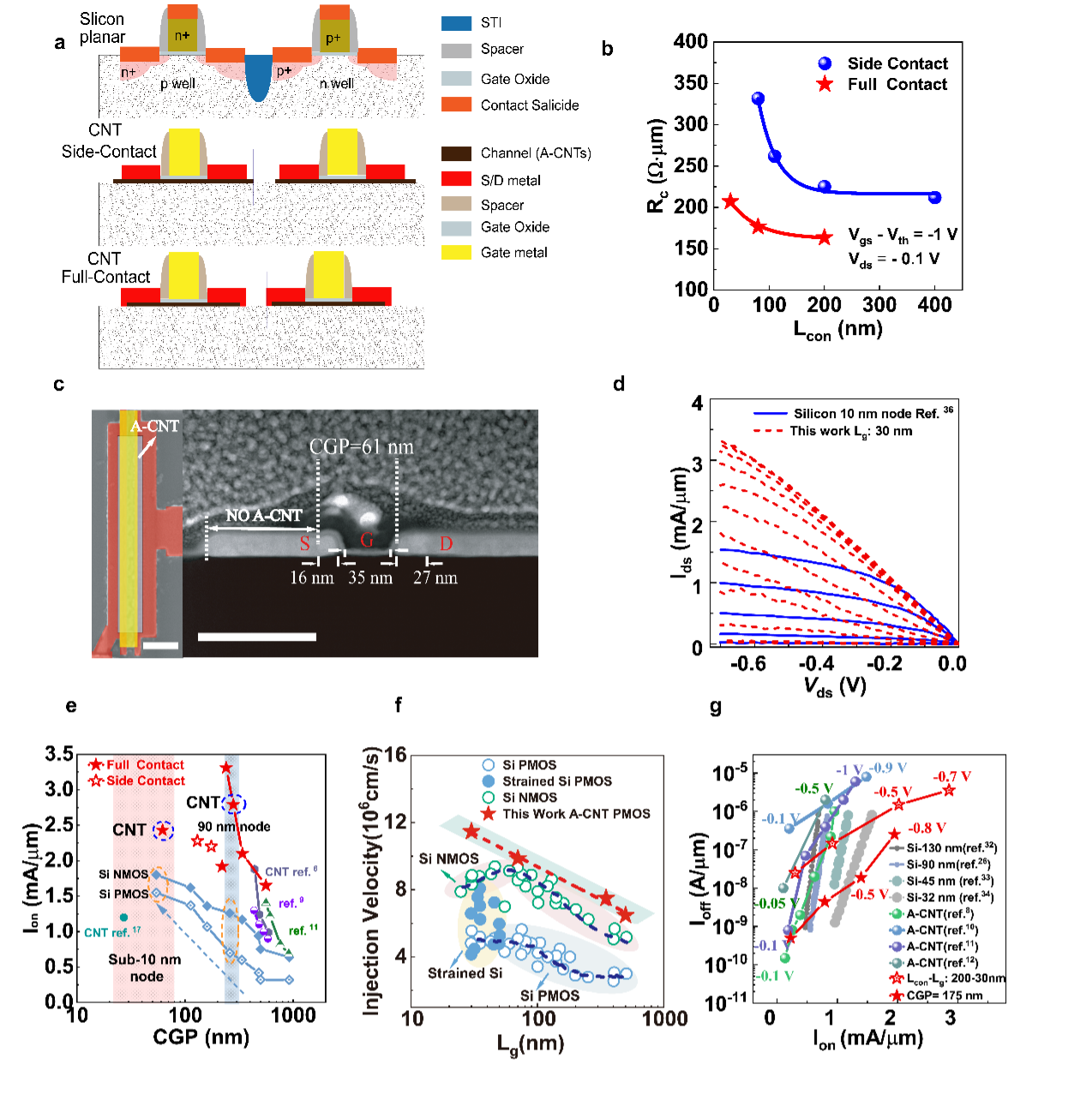
To further scale the sizes of A-CNT transistors, we introduced a full-contact structure between source/drain contacts and nanotubes. The full-contact structure combined the carrier injection mechanism of side contact and end contact,i.e., the carriers can be injected from the contacts to CNTs at both the side (length-dependent) and the edge (length-independent). Therefore, the A-CNT/metal junction in the full-contact structure exhibited lower contact resistance (~90 Ω∙μm) and a weaker dependence on contact length. This enables A-CNT transistors to be further scaled to a CGP of 55 nm, corresponding to silicon 10 nm technology node. Meanwhile, these A-CNT devices also outperformed 10 nm node silicon transistors due to the high carrier mobility and injection velocity of nanotubes. These results illustrated the great potential of A-CNTs for high-performance digital integrated circuits of advanced technology nodes (Fig.3).

Figure 3. Sub-10 nm A-CNT transistors with full-contact structure
More details of this study can be found in “Scaling aligned carbon nanotube transistors to a sub-10 nm node” published inNature Electronics6, 506–515, 2023 (https://www.nature.com/articles/s41928-023-00983-3). Dr. Yanxia Lin from Academy for Advanced Interdisciplinary Studies, Peking University, and Associate Prof. Yu Cao from School of Electronics and Research Center for Carbon-based Electronics, Peking University are first authors and contributed equally to this work. Prof. Lian-mao Peng and Prof. Zhiyong Zhang from School of Electronics and Research Center for Carbon-based Electronics, Peking University, and Beijing Institute of Carbon-based Integrated Circuits are the corresponding authors of this work. Prof. Chuanhong Jin from Zhejiang University and Dr. Lin Xu from Hongkong University are the collaborators of this work.
This work is supported by the National Key Research & Development Program, Natural Science Foundation of China, Beijing Municipal Science and Technology Commission, and Key Laboratory for the Physics and Chemistry of Nanodevices, Peking University.


